Contact
Panel-Level Packaging Solutions​
Panel-level packaging adapts wafer-level techniques from round wafers to square panels, maximizing area utilization and throughput. High-density RDL metallization and interconnect design ensure reliable connections across substrates and materials, improving scalability, flexibility, and manufacturing efficiency.​
RDL Metallization: The Core of High- Density Integration and Signal Transmission​
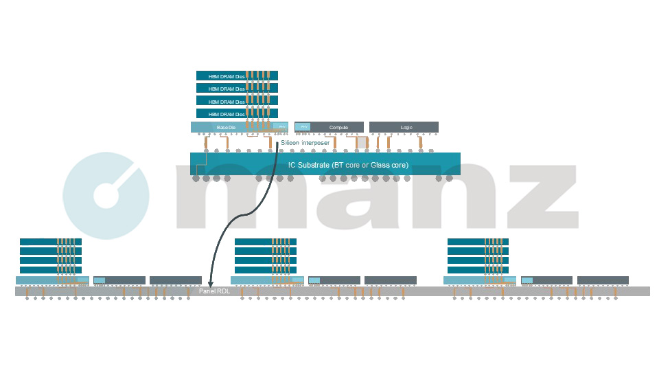
The key to high-density integration in advanced packaging is RDL (Redistribution Layer) technology. As the interconnect between die and substrate, RDL redistributes die I/O, shortens signal paths, and creates compact electrical connections—significantly enhancing high-speed, high-frequency signal performance and stability for RFICs, AI, 5G components, and HPC applications. By enabling localized interconnects and moving beyond traditional PCB/substrate processes to thin-film technologies and advanced 2.5D/3D architectures, RDL supports higher functional density and heterogeneous integration in packaging.​
Panel-Level Packaging RDL Solutions Targeting Both Chip-First and Chip-Last Techniques​
In the Chip-First process, chips are attached to the carrier before the redistribution layer (RDL) is formed. This approach is well suited for smaller, simpler devices—such as PMICs and RF ICs.​

In the Chip-Last process, chips are attached after the RDL structure has been completed. This method is ideal for higher- density, larger-chip applications, such as AI chips and high- performance computing (HPC) processors.​

Panel-level packaging that supports both processes delivers optimal performance with high efficiency and low cost. This framework also enables the packaging industry to meet the diverse needs of heterogeneous integration and high-frequency, high- performance applications.​
Coreless Panel-Level Packaging​ Ultra-thin × Electro-thermal Management​
Designed for PMICs, RFICs and similar devices, panel-level packaging adopts a coreless structure to achieve ultra-thin, compact packages. Using RDL (redistribution layer) to directly connect dies, enabling high-density 10 µm - 30 µm, shortening signal paths and reducing energy loss.​

Additionally, the coreless design lowers thermal resistance and improves heat dissipation, making it ideal for communications and high-performance applications with stringent thickness and thermal requirements. It offers a flexible, high-efficiency advanced packaging solution.​
High-Density Panel-Level Packaging — Large Dies × Fine-Line Interconnects​
PLP for AI and HPC overcomes line/space limits to boost capacity and performance of large AI chips.​

As AI chip designs grow more complex and die sizes increase, wafer-level packaging faces constraints in area utilization. Panel-level
packaging breaks these limits by enabling <10 µm line/space interconnects for higher routing density and more flexible substrate designs, while significantly increasing production throughput.​

A 700 × 700 mm panel holds about eight times more packages than a 12- inch wafer, cutting costs while boosting throughput and area utilization.​

Importantly, this technology supports multi-die integration and heterogeneous chip sizes to meet diverse market needs—making it
especially suitable for AI and HPC applications.​
  • RDL-enabled high-density interconnects.​
  • Significant increases in throughput and area utilization.​
  • Supports both chip-first (RFIC) and chip-last (AI chip) process flows.​
  • Delivers thinner package profiles, enhanced thermal performance, and reduced manufacturing costs.​
  • Panel-level packaging production equipment solutions — validated as a proven route to mass production.​
RDL Metallization: The Core of High- Density Integration and Signal Transmission​
Contact us
Manz Asia
Manz Taiwan Ltd. 4F, No. 168-1, Zhongyuan Rd. 320021 Taoyuan City Taiwan
+886 3 4529811
info.tw@manz.com