Contact
The optimal solution for your market
All markets
Markets
FOPLP
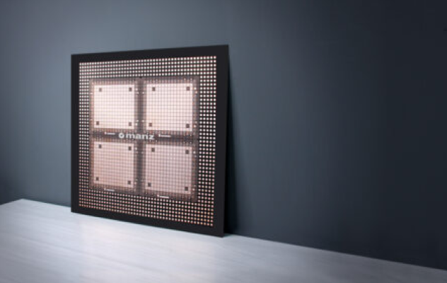
Panel-level packaging adapts wafer-level techniques from round wafers to square panels, maximizing area utilization and throughput. High-density RDL metallization and interconnect design ensure reliable connections across substrates and materials, improving scalability, flexibility, and manufacturing efficiency.​
Markets
IC substrate and Glass Core
With the rapid growth of demand for AI and HPC chip testing, probe cards have become a key factor in overall test yield. We provide a comprehensive range of wet process equipment, covering surface treatment, development, etching, stripping, and plating, to help customers manufacture MLO probe card substrates and achieve higher reliability and competitiveness in semiconductor testing. Meanwhile, we are expanding into next-generation advanced packaging materials with equipment solutions for glass substrates. Leveraging their excellent flatness and thermal stability, our solutions enable higher-density interconnects and superior chip performance for the AI era.
Markets
Digital Printing
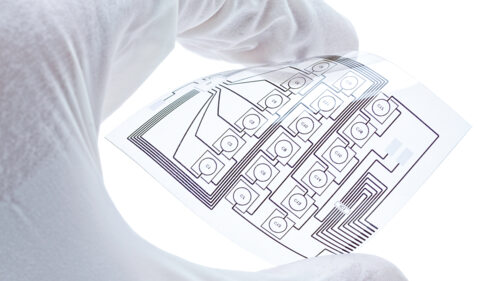
Whether functional or direct-to-product, direct-to-object or even direct-to-shape printing. It's all about high-quality and, above all, direct printing and finishing of products, components and surfaces. As part of its comprehensive technology portfolio, Manz Asia offers engineering solutions for the industrialization of digital printing using inkjet printing technology.
Markets
Contract Manufacturing
With innovative ideas, our expert teams with decades of know-how, as well as state-of-the-art and extremely well-equipped production facilities in Europe and Asia we are a leading high-tech partner for semiconductor, medical devices, precision equipment (such as food-related systems), systems engineering,and parts manufacturing for a variety of customers in various branches.
The right technologies and services to achieve your goals
Products
Cleaning, Developing, Etching, Stripping
Manz Asia provides cleaning, development, etching, and stripping process equipment, primarily used in the production of semiconductor panel-level packaging (PLP), advanced IC substrates (glass substrates & probe card MLO), and displays.
Products
Desmear (DSM) & Plating Through Hole (PTH)
Our continuous horizontal DSM&PTH equipment, purpose-built for high-aspect-ratio AI server PCB production, together with our gantry-type DSM&PTH designed specifically for probe card MLO manufacturing, jointly provide a complete and reliable solution to meet the stringent process requirements of today’s advanced electronic products.
Products
ECD
The key technology to achieve the RDL process in Panel Level Packaging , Through Glass Vias (TGV) and Probe card MLO.
Products
Inkjet Printing
Inkjet printing plays a decisive role in the field of semiconductor IC packaging and offer numerous advantages. With our state-of-the-art printing systems, we enable increased flexibility in your production and significantly improve the environmental friendliness of your system.
Products
Automation
With thousands of robotic systems installed worldwide, Manz Asia is a trusted partner for intelligent automation in display, PCB, and semiconductor panel-level packaging industries.
Our proven expertise in handling and robotics empowers customers to achieve higher precision, faster throughput, and greater manufacturing efficiency.
All products
News & Reports
2026-09-03
Manz Asia and SUSS Announce Strategic Collaboration in Semiconductor Inkjet Technology
• Combining Manz Asia’s inkjet and manufacturing expertise with SUSS’ semiconductor process capabilities Driving next-generation inkjet solutions for advanced and panel-level packaging applications Accelerating the transition of inkjet technology toward high-volume semiconductor manufacturing Taoyuan, Taiwan, September 3, 2026 – A leading semiconductor advanced packaging equipment manufacturer, Manz Asia, today announced a strategic collaboration with SUSS, a leading manufacturer of equipment and process solutions for the semiconductor industry, to jointly advance next-generation inkjet solutions for semiconductor manufacturing and advanced packaging applications. As semiconductor manufacturing moves toward higher integration, more complex structures and larger-format processing, manufacturers are seeking greater process flexibility, material efficiency and manufacturing scalability. Inkjet printing is gaining increasing attention as an enabling technology to address these requirements. Compared with conventional coating approaches, inkjet technology enables precise and selective material deposition, reduces material consumption and can simplify process flows, creating new opportunities across advanced packaging and other high-value semiconductor manufacturing applications. A key focus of the collaboration will be to jointly explore new inkjet applications, validate materials and processes, and develop scalable manufacturing approaches. Manz Asia contributes proven inkjet capabilities, manufacturing engineering expertise and a strong position in the panel-level packaging ecosystem, supported by an end-to-end inkjet development platform and a Lab-to-Fab approach spanning material and substrate preparation, printing, curing and process characterization. SUSS brings deep semiconductor process expertise and global customer reach. Together, these complementary capabilities enable Manz Asia and SUSS to systematically evaluate and optimize processes, accelerate development and identify solutions tailored to specific semiconductor applications. The companies aim to shorten time-to-market and accelerate the transition of inkjet technology from advanced process development toward high-volume semiconductor manufacturing. "Successfully commercializing new semiconductor technologies requires deep process expertise, strong application know-how and close alignment with customer roadmaps. By combining SUSS' semiconductor process experience with Manz Asia's inkjet expertise, we can accelerate technology development and reduce time-to-market for future solutions. At the same time, the collaboration strengthens our access to the emerging panel-level packaging ecosystem, an area we believe will play an increasingly important role in next-generation semiconductor manufacturing. This partnership supports our Ambition 2030 strategy by strengthening our technology portfolio, expanding our capabilities in advanced packaging and increasing our exposure to attractive semiconductor growth markets", said Burkhardt Frick, CEO of SUSS. “Panel-level packaging is entering a new phase, driven by higher integration and increasingly complex structures. These developments are creating new demands for greater process flexibility, material efficiency and manufacturing scalability. Through our collaboration with SUSS, Manz Asia is combining its inkjet printing and manufacturing expertise with SUSS' semiconductor process capabilities and global customer reach. Together, we see strong potential to accelerate the transition of inkjet technology from advanced process development toward high-volume semiconductor manufacturing. This collaboration marks an important step toward delivering scalable, next-generation solutions for advanced packaging and future semiconductor applications,” said Robert Lin, CEO of Manz Asia. About Manz Asia Manz Asia delivers semiconductor equipment and solutions built on core technologies in Electrochemical Deposition (ECD), wet chemistry, digital printing, automation, and software integration. Our expertise covers advanced packaging (FOPLP / CoPoS) and IC substrate processing (glass and organic core), supporting customers from R&D to high-volume manufacturing. Through system solutions, contract manufacturing, and sales representation, we help customers accelerate time-to-market, boost yield, and stay competitive in the fast-evolving semiconductor industry. For more information, visit www.manz.com.tw About SUSS SUSS is a leading global provider of equipment and process solutions for the semiconductor industry. Focused on cutting-edge technology and precision engineering, we enable the production of next-generation microchips and semiconductor devices that power digital progress. Developed in close collaboration with research institutes and industry partners, our solutions fuel the AI and high-performance computing ecosystem and shape the future of intelligent devices and applications worldwide. Headquartered in Garching, Germany, SUSS has approximately 1,500 employees worldwide and recently generated sales of approximately €500 million. We operate production sites in Germany and Taiwan and development centers in Europe, Asia and the US, supported by a strong network of sales and service offices with close proximity to our customers. SUSS MicroTec SE is listed on the Frankfurt Stock Exchange (Prime Standard, FWB: SMHN; ISIN DE000A10K0235) and is part of the TecDAX and MDAX indices. For more information, visit www.suss.com. Contact: Manz Taiwan Ltd. Yvonne Huang Director of Marketing & Communications Phone: +886 3 452 9811 ext. 3399 E-Mail: yvonne.huang@manz.com
2026-08-18
Manz Asia Pioneers Production-Proven 310/510/700 mm ECD and Wet Process Solutions for Panel-Level Packaging
• Enabling scalable RDL manufacturing for CoPoS, FOPLP and Glass Core TGV applications Taoyuan, Taiwan – August 18, 2026 – Manz Asia, a leading provider of semiconductor advanced packaging equipment and process solutions, has pioneered production-proven ECD (electrochemical deposition) platforms supporting 310 mm, 510 mm, and 700 mm panel formats. Building on ECD as a core technology, Manz Asia integrates key wet process tools—including cleaning, developing, etching, and stripping—into the Omni 310, Omni 510, and Omni 700 platforms to enable scalable panel-level RDL manufacturing. Extending RDL Process Value from Established Applications to Next-Generation Advanced Packaging As AI and advanced computing drive increasingly complex chiplet-based architectures, larger interposers and substrates are becoming essential to integrate more heterogeneous components within a single package. This evolution is accelerating the shift from 300 mm wafer-based manufacturing toward larger panel formats, while increasing the importance of RDL in enabling high-density interconnects across increasingly complex package architectures. With expertise spanning equipment and process integration, Manz Asia addresses evolving RDL manufacturing requirements by integrating ECD and key wet processes within a unified equipment portfolio. This approach helps manufacturers simplify process integration, reduce the complexity of managing multiple equipment suppliers, and gain greater flexibility across panel sizes and advanced packaging architectures. The Omni Series supports advanced packaging applications including FOPLP, CoPoS, and Glass Core TGV, with proven applications for PMIC and RF devices for communication and automotive markets. The platform also provides a foundation for continued technology development toward emerging AI and HPC packaging requirements. Glass Core TGV Process Enabling High-Performance Interconnects As Glass Core gains momentum in next-generation advanced packaging, TGV (Through-Glass Via) manufacturing requires precise glass micromachining, microvia formation, metallization, and high-aspect-ratio filling. Manz Asia is extending its etching and ECD technologies to address these requirements. Its glass etching equipment supports substrates up to 0.4 mm thick and microvias down to 20 μm, with TGV structures featuring aspect ratios of up to 1:20, enabling precise and controlled via formation. For TGV metallization, Manz Asia’s ECD technology supports high-aspect-ratio via filling and can be integrated with seed-layer sputtering and plating chemistry to enable void-free copper filling and uniform metal deposition. This integrated approach addresses critical requirements for fill quality, plating uniformity, and structural reliability in Glass Core TGV manufacturing. Advancing Panel-Level Packaging from Innovation to Production “AI-driven semiconductor growth is accelerating the evolution of advanced packaging, driving greater integration, larger package formats, and increasingly complex interconnect architectures,” said Robert Lin, CEO of Manz Asia. “RDL is becoming a critical enabling technology, connecting chips, interposers, substrates, and PCBs across emerging architectures such as CoPoS, FOPLP, and Glass Core TGV.” “Our 310 mm, 510 mm, and 700 mm production-proven RDL platforms reflect our commitment to scalable manufacturing across diverse package architectures and substrate formats,” Lin continued. “With a broad portfolio covering most of the key process steps in RDL manufacturing, Manz Asia enables customers to streamline supplier coordination, simplify process integration, and deploy more efficient production solutions.” “Manz Asia’s role goes beyond equipment delivery. We work closely with customers to bridge the gap between process innovation and high-volume manufacturing, with a focus on productivity, yield, and cost performance. By combining process expertise, equipment integration, and continuous innovation, we aim to accelerate the adoption of panel-level packaging and contribute to a more robust advanced packaging ecosystem for the AI era.” ▲Manz Asia Omni Series – ECD and Wet Process Platform for Scalable Panel-Level RDL Manufacturing About Manz Asia Manz Asia delivers semiconductor equipment and solutions built on core technologies in Electrochemical Deposition (ECD), wet chemistry, digital printing, automation, and software integration. Our expertise covers advanced packaging (FOPLP / CoPoS) and IC substrate processing (glass and organic core), supporting customers from R&D to high-volume manufacturing. Through system solutions, contract manufacturing, and sales representation, we help customers accelerate time-to-market, boost yield, and stay competitive in the fast-evolving semiconductor industry. www.manz.com.tw/en
All News
Dates & Events
03/25/2026 - 03/27/2026
SEMICON China 2026
SNIEC | Shanghai,China
04/08/2026 - 04/10/2026
Touch Taiwan 2026
TaiNEX | Taipei, Taiwan
All Events
Driving Technological Innovation Today to Shape the Future
read more