Contact
The optimal solution for your market
All markets
Markets
FOPLP
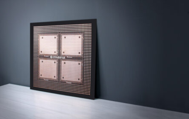
Panel-level packaging adapts wafer-level techniques from round wafers to square panels, maximizing area utilization and throughput. High-density RDL metallization and interconnect design ensure reliable connections across substrates and materials, improving scalability, flexibility, and manufacturing efficiency.​
Markets
IC substrate and Glass Core
With the rapid growth of demand for AI and HPC chip testing, probe cards have become a key factor in overall test yield. We provide a comprehensive range of wet process equipment, covering surface treatment, development, etching, stripping, and plating, to help customers manufacture MLO probe card substrates and achieve higher reliability and competitiveness in semiconductor testing. Meanwhile, we are expanding into next-generation advanced packaging materials with equipment solutions for glass substrates. Leveraging their excellent flatness and thermal stability, our solutions enable higher-density interconnects and superior chip performance for the AI era.
Markets
Digital Printing
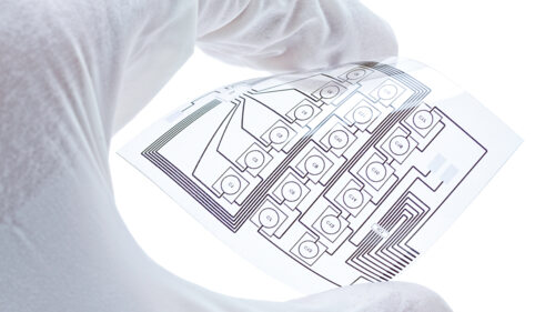
Whether functional or direct-to-product, direct-to-object or even direct-to-shape printing. It's all about high-quality and, above all, direct printing and finishing of products, components and surfaces. As part of its comprehensive technology portfolio, Manz Asia offers engineering solutions for the industrialization of digital printing using inkjet printing technology.
Markets
Contract Manufacturing
With innovative ideas, our expert teams with decades of know-how, as well as state-of-the-art and extremely well-equipped production facilities in Europe and Asia we are a leading high-tech partner for semiconductor, medical devices, precision equipment (such as food-related systems), systems engineering,and parts manufacturing for a variety of customers in various branches.
The right technologies and services to achieve your goals
Products
Cleaning, Developing, Etching, Stripping
Manz Asia provides cleaning, development, etching, and stripping process equipment, primarily used in the production of semiconductor panel-level packaging (PLP), advanced IC substrates (glass substrates & probe card MLO), and displays.
Products
Desmear (DSM) & Plating Through Hole (PTH)
Our continuous horizontal DSM&PTH equipment, purpose-built for high-aspect-ratio AI server PCB production, together with our gantry-type DSM&PTH designed specifically for probe card MLO manufacturing, jointly provide a complete and reliable solution to meet the stringent process requirements of today’s advanced electronic products.
Products
ECD
The key technology to achieve the RDL process in Panel Level Packaging , Through Glass Vias (TGV) and Probe card MLO.
Products
Inkjet Printing
Inkjet printing plays a decisive role in the field of semiconductor IC packaging and offer numerous advantages. With our state-of-the-art printing systems, we enable increased flexibility in your production and significantly improve the environmental friendliness of your system.
Products
Automation
With thousands of robotic systems installed worldwide, Manz Asia is a trusted partner for intelligent automation in display, PCB, and semiconductor panel-level packaging industries.
Our proven expertise in handling and robotics empowers customers to achieve higher precision, faster throughput, and greater manufacturing efficiency.
All products
News & Reports
2026-06-15
Manz Asia Successfully Delivers World’s First 310mm × 310mm Panel-Level Packaging ECD Production System
• World’s first 310mm × 310mm panel-level packaging (PLP) Electrochemical Deposition (ECD) production system delivered to customer line Omni X-series covering 310mm, 510mm, and 700mm platforms, enabling a broad range of panel-level manufacturing applications. Supports FOPLP, CoPoS, and TGV applications for AI, HPC, and advanced memory markets Taoyuan, Taiwan, June 15, 2026 – A leading semiconductor advanced packaging equipment manufacturer, Manz Asia, has successfully delivered the world’s first 310mm × 310mm panel-level packaging (PLP) Electrochemical Deposition (ECD) mass production system. The system expands Manz Asia’s advanced packaging portfolio and showcases its integrated in-house expertise in process innovation, equipment engineering, and high-volume manufacturing. The new ECD platform is designed with high flexibility to support both glass and metal square carriers and integrates wet chemical process modules for Redistribution Layer (RDL) fabrication. It is engineered for FOPLP-, CoPoS-, and TGV-based advanced packaging architectures. The 310mm × 310mm format offers advantages in scalability, panel utilization, and production yield, positioning it as a key enabling technology for panel-level packaging to support AI, high-performance computing (HPC), high-bandwidth memory (HBM), and high-speed interconnect applications. Advanced packaging is increasingly converging with leading-edge semiconductor process technologies, with manufacturing capacity progressively concentrated in Taiwan. This shift is accelerating integration across process nodes and packaging architectures in the global semiconductor supply chain. Leveraging strong in-house R&D capabilities and close collaboration with leading IDM and packaging customers, Manz Asia continues to accelerate technology iteration and volume production deployment, strengthening its position in the global panel-level packaging equipment ecosystem. The ECD system seamlessly integrates a full suite of wet chemical process modules, including cleaning, developing, etching, and stripping, and supports both spin and spray processing modes, creating a comprehensive 310mm × 310mm panel-level RDL manufacturing solution under the “Omni 310” platform. The Omni X-series now spans Omni 310 (310mm × 310mm), Omni 510 (510mm × 515mm), and Omni 700 (700mm × 700mm), forming a scalable platform architecture for panel-level mass production. The modular system design enables flexible configuration across different device architectures, process flows, and production capacity requirements, supporting development, qualification, pilot production, and high-volume manufacturing. It strengthens Manz Asia’s competitiveness in the global advanced packaging equipment market. Robert Lin, CEO of Manz Asia, said the successful deployment of the Omni 310 into customer production lines reflects growing market demand for advanced packaging platforms that combine flexibility with production readiness. “As advanced packaging becomes increasingly central to AI and high-performance computing (HPC) architectures, capabilities such as process control, scalability, and seamless integration into high-volume manufacturing environments have become key competitive differentiators,” he said. He added that Manz Asia will continue to advance its technology roadmap as a global-class equipment supplier, further strengthening its integration of ECD and wet chemical process technologies to improve manufacturing efficiency, yield stability, and production ramp-up. “We aim to accelerate the deployment of next-generation packaging technologies in FOPLP, CoPoS, and TGV, while reinforcing supply chain resilience across the semiconductor ecosystem,” he said. “Through a multi-platform strategy spanning 310mm, 510mm, and 700mm, we provide a consistent technology pathway from process development to high-volume manufacturing, enabling customers to scale efficiently and predictably. The Omni X-series roadmap is designed to support sustainable and scalable capacity expansion for next-generation semiconductor packaging applications.” ▲ Manz Asia World’s First 310mm × 310mm Panel-Level Packaging ECD Production System About Manz Asia Manz Asia delivers semiconductor equipment and solutions built on core technologies in Electrochemical Deposition (ECD), wet chemistry, digital printing, automation, and software integration. Our expertise covers advanced packaging (FOPLP / CoPoS) and IC substrate processing (glass and organic core), supporting customers from R&D to high-volume manufacturing. Through system solutions, contract manufacturing, and sales representation, we help customers accelerate time-to-market, boost yield, and stay competitive in the fast-evolving semiconductor industry. www.manz.com.tw/en Contact: Manz Taiwan Ltd. Yvonne Huang Director Marketing & Communications Phone: +886 3 452 9811 ext. 3399 E-Mail: yvonne.huang@manz.com
2026-03-12
Manz Asia and Epson Form Strategic Partnership to Advance Inkjet Technology for Semiconductor Manufacturing
• Joint Lab-to-Fab inkjet equipment combines Epson’s precision printhead technology with Manz Asia’s equipment and process expertise to enable scalable manufacturing Taoyuan, Taiwan — March 12, 2026 — A leading semiconductor advanced packaging equipment manufacturer Manz Asia today announced a strategic partnership with Seiko Epson Corporation (Epson) aimed at accelerating the adoption of advanced inkjet technology in semiconductor manufacturing. The collaboration combines Manz Asia’s expertise in semiconductor equipment engineering, process integration, and intelligent software systems with Epson’s industry-leading inkjet printhead technology. By bringing together these complementary capabilities, the two companies are developing scalable Lab-to-Fab inkjet equipment designed to support next-generation semiconductor manufacturing applications. The jointly developed inkjet equipment is available as a series of systems covering R&D, pilot production, and mass manufacturing, enabling semiconductor manufacturers to expand applications, validate materials efficiently, optimize process parameters, and scale seamlessly from development to high-volume production. Manz Asia’s inkjet system solutions with high compatibility features enable precise 2D and 3D printing of conductive, photoresist, and specialized functional inks on a variety of products, components, and surfaces. The systems are well-suited for key semiconductor processes, including patterning 2.5D/3D antenna traces, heatsink layers, and bonding layers for RFIC, PMIC, and CPO devices. All of these applications can be handled with Manz Asia inkjet system solutions, providing flexible, scalable, and cost-effective solutions for advanced packaging and emerging device architectures. Robert Lin, CEO of Manz Asia, said: “Inkjet technology is transforming semiconductor manufacturing. Together with Epson, we are delivering precise and scalable inkjet equipment solutions that enable manufacturers to validate processes and scale from R&D to high-volume production. Our Taiwan R&D center serves as an open innovation hub, uniting materials partners, printhead providers, and key suppliers, turning innovative concepts into practical manufacturing outcomes and helping customers achieve faster time-to-market and improved production efficiency.” Shunya Fukuda, COO of Epson’s IJS Operations Division, added: “Digital additive manufacturing using inkjet technology is expected to become a key technology supporting the evolution of semiconductor packaging. By leveraging Epson’s high-precision droplet control technology and volume production know-how developed, we works together with Manz Asia to build a scalable manufacturing platform bridging laboratory development and volume production. Through this initiative, Epson aims to contribute to the sustainable development of the semiconductor industry.” This collaboration marks a step toward more flexible, efficient, and sustainable semiconductor production, leveraging complementary core technologies to deliver long-term differentiation and measurable value to global customers. Picture 1: RDJet100 ─ a laboratory equipment for validating new functional inks and substrates in semiconductor advanced packaging metallization process. Powered by Epson printhead. Picture 2: ICJet series ─ Industrial production equipment for frontend and backend semiconductor processes, supporting wafer and panel substrates. Picture 3: Manz Asia and Epson have teamed to deliver inkjet system solutions for semiconductor processes—2.5D/3D antennas traces, heatsinks, and bonding layers for RFIC/PMIC/CPO—enabling transformative production advances. About Manz Asia Manz Asia delivers semiconductor equipment and solutions built on core technologies in wet chemistry, plating, inkjet printing, automation, and software integration. Our expertise covers advanced packaging (High-Density PLP / FOPLP) and IC substrate processing (glass and organic core), supporting customers from R&D to high-volume manufacturing. Through system solutions, contract manufacturing, and sales representation, we help customers accelerate time-to-market, boost yield, and stay competitive in the fast-evolving semiconductor industry. www.manz.com.tw/en About SEIKO EPSON Epson is a global technology leader whose philosophy of efficient, compact, and precise innovation enriches lives and helps create a better world. Epson is focused on solving societal challenges through innovations in printing, manufacturing, and visual technologies, with the goal of becoming carbon negative and eliminating the use of exhaustible underground resources by 2050.Led by Seiko Epson Corporation, the Epson Group generates annual sales of more than JPY 1 trillion. corporate.epson/en/ Contact: Manz Taiwan Ltd. Yvonne Huang Director Marketing & Communications Phone: +886 3 452 9811 ext. 3399 E-Mail: yvonne.huang@manz.com
All News
Dates & Events
03/25/2026 - 03/27/2026
SEMICON China 2026
SNIEC | Shanghai,China
04/08/2026 - 04/10/2026
Touch Taiwan 2026
TaiNEX | Taipei, Taiwan
All Events
Driving Technological Innovation Today to Shape the Future
read more